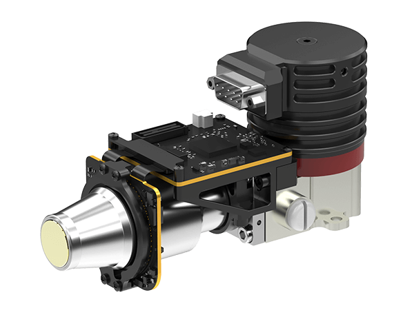
Uncooled infrared detector is the core component of uncooled thermal imaging system. It takes advantage of the basic rule that all objects above absolute zero will radiate infrared energy outward. It uses sensitive element materials to absorb the radiation energy of the target and convert it into heat energy. The change of heat energy changes the physical properties of the sensitive element, and then converts the object through a specially designed conversion mechanism. The change of physical properties is converted into electrical signal to realize the detection and measurement of the target.
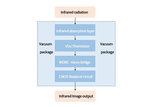
The most commonly used thermal sensitive materials include vanadium oxide (VOX), amorphous silicon (a-Si), silicon diode and so on. The uncooled infrared detector developed by Global Sensor Technology mainly uses vanadium oxide (VOX) material, which has high TCR (resistance temperature coefficient, about 2% / K ~ 3% / k at room temperature) and high sensitivity.
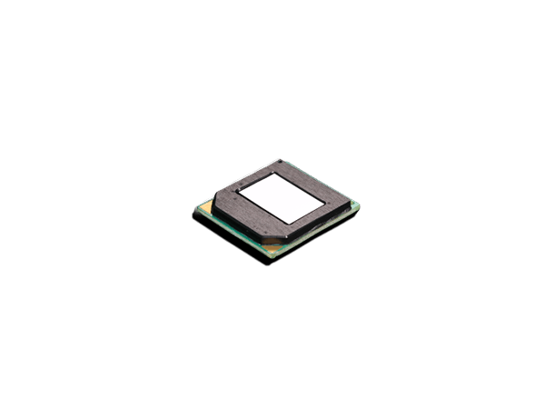
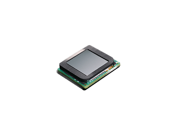
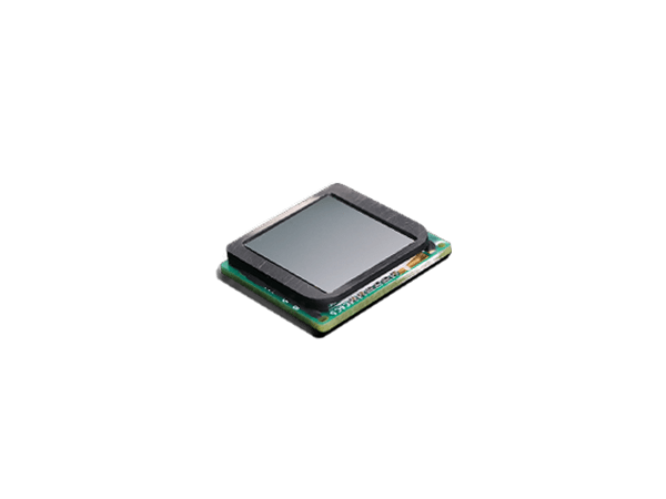
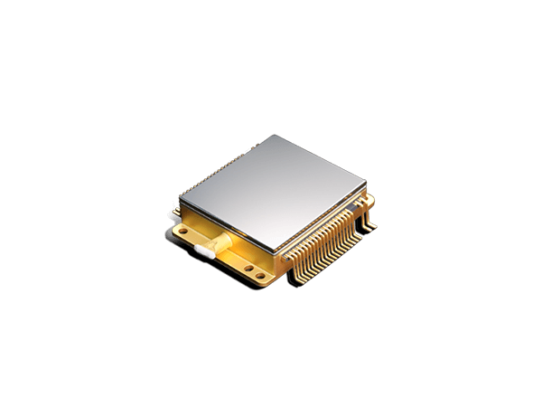
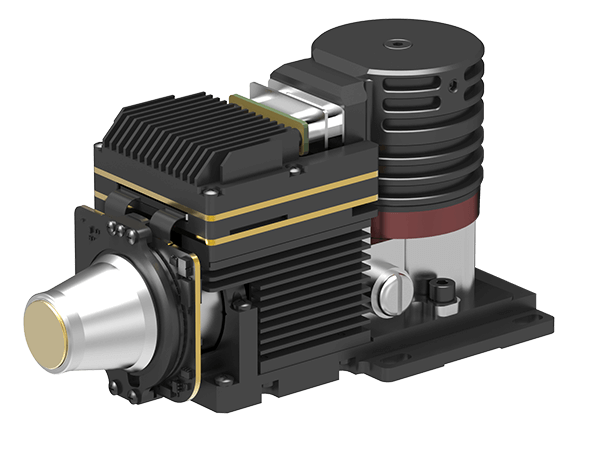
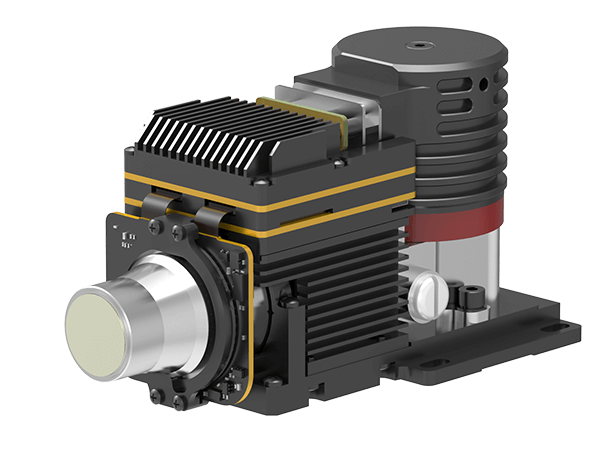
At present, the packaging process of uncooled infrared detector in the industry mainly includes metal packaging, ceramic packaging and wafer level packaging.
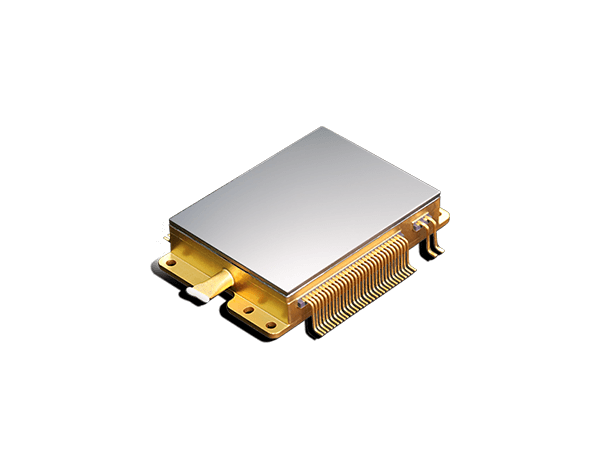
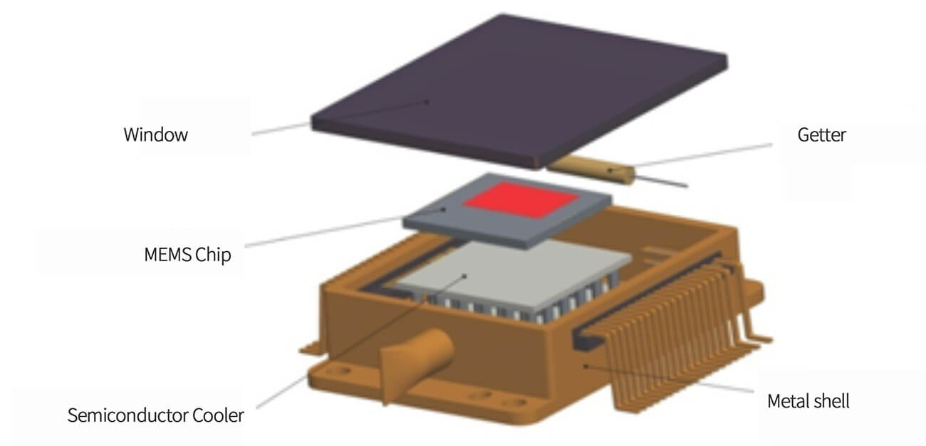
Metal packaging is the earliest packaging format in the industry. In the fabrication process of metal encapsulated uncooled infrared detector, firstly, the wafer of the readout circuit is processed, and the MEMS Micro bridge structure is grown at the reserved interface of the readout circuit, and then sliced. The detector chip on the whole wafer is cut into independent die, and then each die is connected with the metal shell, TEC, getter and infrared protection window. The vacuum packaging and related tests are completed. Metal packaged detector has the best imaging stability, environmental adaptability and reliability among the three packaging forms, but its components are expensive and its manufacturing cost is high, so it is more suitable for high-end or special field applications.
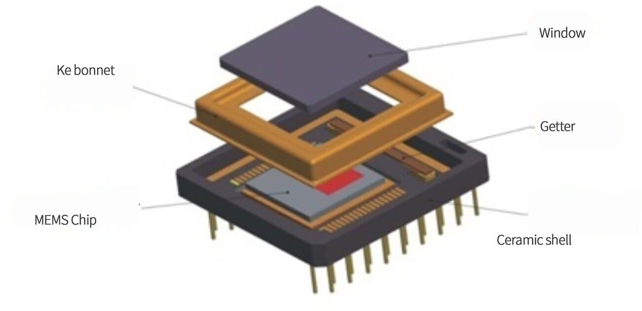
Ceramic packaging process is similar to metal packaging, which is a mature infrared detector packaging technology. Compared with metal packaging, the volume and weight of the packaged detector will be greatly reduced. The cost of raw materials and manufacturing is lower than that of traditional metall packaging, which is suitable for mass production of electronic components. The development of ceramic shell packaging technology benefits from the improvement of readout circuit performance and the increasingly perfect Tecless technology. Without TEC, it can reduce the requirements of packaging shell volume and reduce the cost, which is more popular in civilian products. However, it still can not meet the application needs of emerging fields such as smart home and consumer electronics.
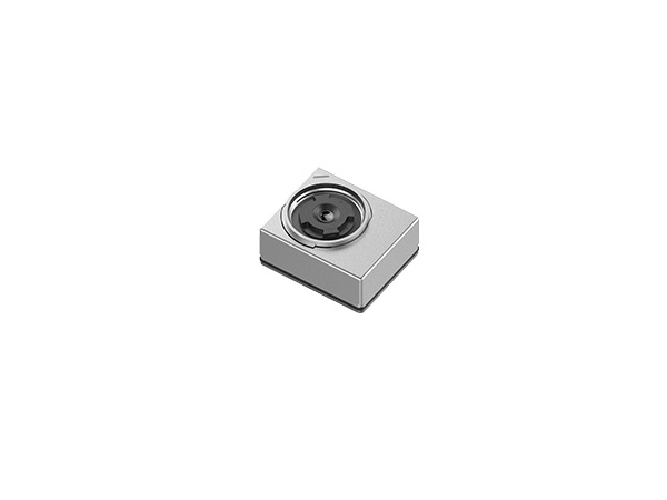
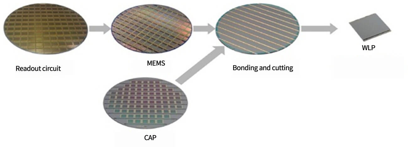
Wafer level packaging is an increasingly mature packaging format in recent years. It needs to manufacture another silicon window wafer corresponding to the microbolometer wafer. The microbolometer wafer and the silicon window wafer are aligned precisely, the infrared detector chip and the silicon window are aligned one by one, and welded together in the vacuum cavity through the solder ring. Finally, the wafer level packaging is completed and the splits become a vacuum sealed wafer level infrared detector. In terms of technology, it can achieve smaller volume, higher efficiency, higher output and lower cost. It can be used in industrial and civil products, and can also be widely used in the field of consumer products, making it possible for infrared thermal imaging technology to enter ordinary people's daily life.
Go Top