Packaging Technology of Uncooled FPA Infrared Detectors
Uncooled infrared detector is the core component of uncooled thermal imaging system. With the rapid development of uncooled thermal detector technology, the technical level and quality of related infrared products have been greatly improved.
At present, the packaging cost has accounted for more than 50% of the total development cost of uncooled thermal imaging detectors, and the main factor that determines the packaging cost is the packaging technology used. So, the cost and reliability of packaging technology is becoming more and more important.
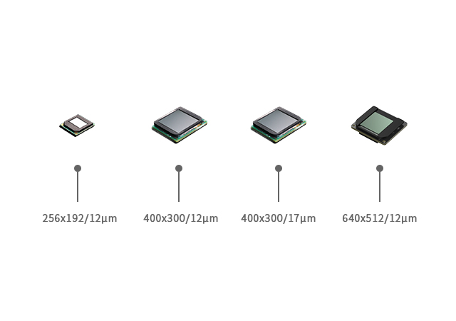
There are three main packaging technologies in the infrared market currently: metal packaging, ceramic packaging and wafer-level packaging. According to their different advantages, they can be applied to different industries.
1.Metal Packaging
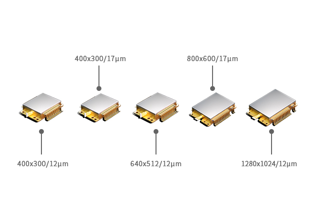
Metal packaging uses metal tube shell, thermoelectric cooler (TEC) and columnar getter. The TEC plays an important role of stabilizing the working temperature so that the infrared detector works at room temperature, thereby improving the ability of thermal imaging sensors to adapt to extreme environments, such as heavy fog, rain and snow etc.
But the disadvantage is that the cost is too high, accounting for more than 60% of the total cost of the entire uncooled products production, and causing a long production cycle. Such packaging method is for high-end applications.
Until now, metal package is still the mainstream way in thermal uncooled infrared detector market. Due to its stable performance and long operating life, metal package thermal detector sensor is widely used in various fields and industries.
The metal packing uncooled VOx microbolometer infrared detectors developed by Global Sensor Technology (GST) includes various resolution from 400x300 to large array 1280x1024 resolution.
Based on metal package technics and TEC technology, GST uncooled infrared microbolometer has high sensitivity, stable performance characteristics and can present clear imaging quality in various kinds of harsh working environment such as total darkness, thick fog, heavy rain, snow, sand storm etc.

2.Ceramic Packaging
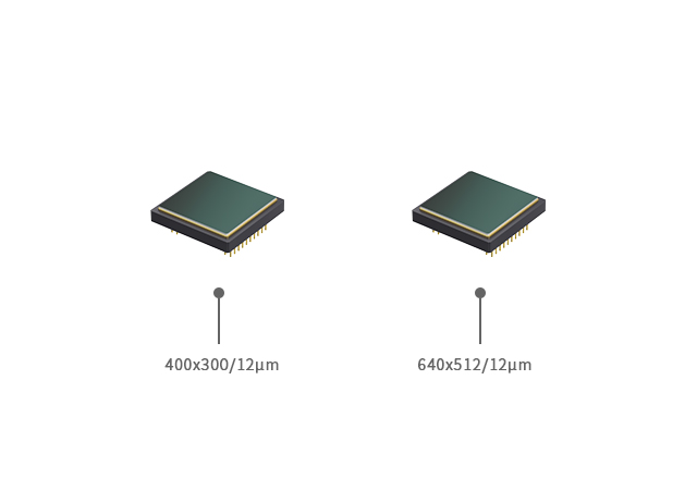
Ceramic packaging process is similar to metal packaging, which is a mature infrared detector packaging technology. Compared with metal packaging, the volume and weight of the packaged detector will be greatly reduced. For ceramic packaging, its readout circuit has self-adjusting operating temperature function and does not require TEC stabilization.
GST ceramic package uncooled infrared detector is a new arrival infrared product developed by Global Sensor Technology. It uses the international mainstream vanadium oxide material which makes it own more outstanding comprehensive performance.
Ceramic packaging is currently the most popular packaging technology on the market. The size, weight and power consumption of the detector can be significantly reduced. By integrating the ceramic packaging infrared detector, the infrared camera could present clear and sharp images.
This new ceramic package infrared detector will give more choices for customers from various industries such as Industrial Automation, Intelligent Security, Unmanned Platform, Robot, Intelligent Hardware, Advanced Driver Assistant System, Firefighting etc.

3.Wafer Level Packaging
Wafer-level packaging, also known as wafer-level size packaging, has become an important part of advanced packaging technology in the semiconductor industry. Wafer level packaging (WLP) is the process of completing high vacuum packaging directly on the entire MEMS wafer, then scribing and cutting to make a single infrared detector. It performs most or all of the packaging and testing procedures directly on the IR detector wafer before dicing. It is an improved chip size package that meets the needs of small size, lightweight, portable, handheld, low price and high production efficiency.
GST wafer-level-package infrared focal plane array (FPA) detector is specially developed for optimized size, weight, power, cost (SWaP-C), which has achieved high volume production with annual output up to 1,000,000 pieces.
Until now, we have provided our customers with various mature and stable infrared thermal imaging solutions. It’s easier for WLP thermal sensors developed by GST to be integrated into more terminal products and greatly reduces the cost for customers.
